I think the documentation, while very long isn't always that clear. It appears comprehensive when you first start working with it but the more I learned the more holes I found.
AD7705 Hardware
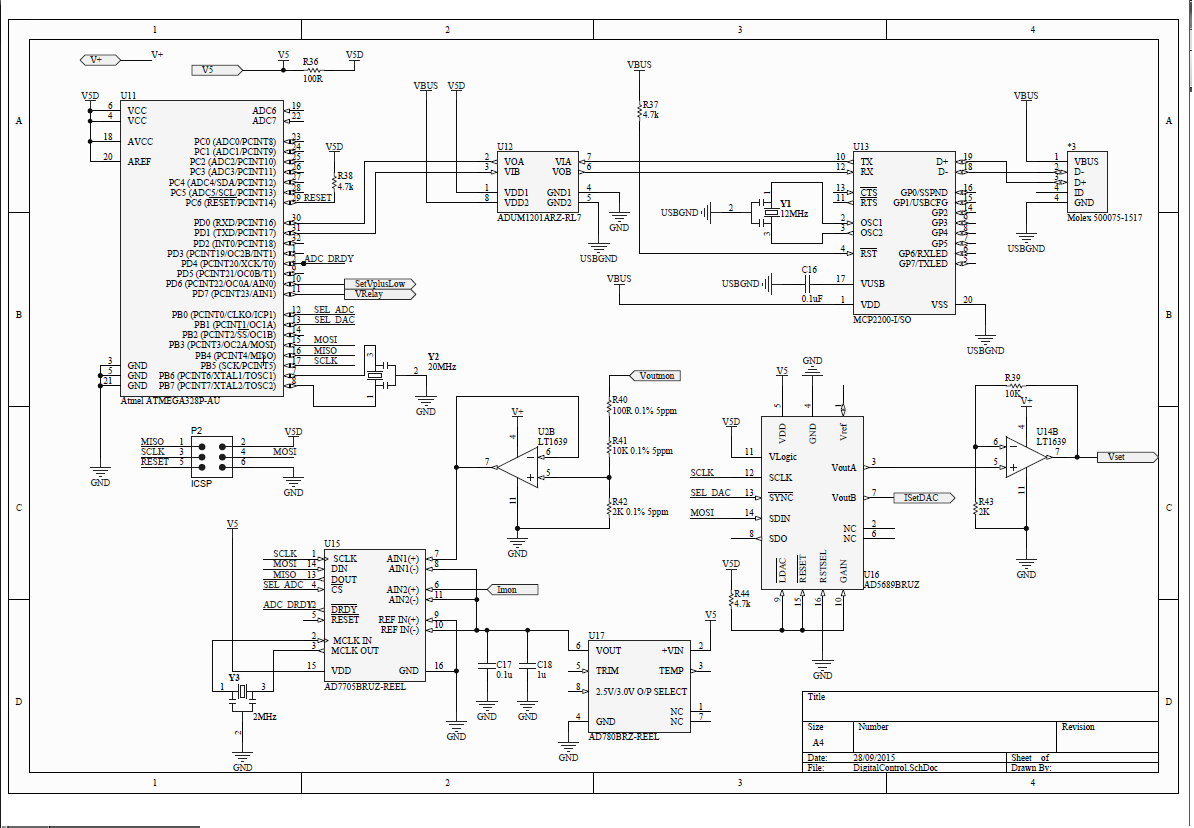
The AD7705 is a 16 bit analog to digital converter of the delta sigma type. It's excellent for low rate, high precision conversions. It has a two differential inputs and is SPI (which is important as the DAC I am using is also SPI). The specs look very impressive with very good linearity and no missing codes.
As I said before - the part has no internal reference so I am using it with an AD780 that I was testing before and which I found impressively stable.
It turns out that to get the full range I need, I have to configure the part to run in bipolar mode. It isn't really bipolar in the sense that both the analog inputs for a given channel have to be above the voltage of the ground line but the AIN(+) can be at a lower voltage than AIN(-). In unipolar mode I can only get a range of zero to the voltage reference (2.5V). To get 0 .. 5V I have to run the part in bipolar mode and connect the AIN(-) line to the reference. Then the AIN(+) can swing from zero (ref-2.5V) to 5V (reg+2.5V). I could run in unipolar mode and scale the input to 0..2.5V but this means the voltage per step is then just 38uV which is starting to look a lot like the noise level.
The part contains an input buffer but if you use this, the input range is restricted to 50mV - VDD -1.5V. This pretty much rules out the buffer for my application since even if I ran it in unipolar mode I need to go lower than 50mV.
The plan is to use one channel to read the output voltage and the second channel to read the current. A voltage divider followed by a unit-gain buffer will scale and buffer the output voltage and there is already a buffer for the current (which doesn't need to be scaled).
The part has a data ready line that goes low when there is data to read. It is also possible to check the status of this line in software. I went back and forth between using the hardware line and using software and am currently using the hardware line. This was mostly as I was having problems though rather than for any real reason.
Programming
SPI Setup
As for the DAC, I used my SPIDevice class as the basis for the ADC code. The first thing is that this device uses a different SPI mode than the DAC. The setup looks like this: setClockPolarity(SPIDevice::CLOCK_POLARITY_FALLING_LEADS);
setClockPhase(SPIDevice::CLOCK_PHASE_SAMPLE_ON_TRAILING);
setDoubleSpeedModeEnabled(true);
setClockRate(SPIDevice::RATE_DIV_DBL_2);
setBitOrdering(SPIDevice::MSB_FIRST);
Registers, Initialisation
The ADC takes more setup than the DACs I used before. The ADC has a bunch of internal registers you can read or write that change it's behaviour or return the result of a conversion. The first byte you send to the part is used to write to the communications register and this allows you to select a register, to indicate if you want to read or write, select the channel you want to work with or put the part in standby mode. You basically write a byte to the communications register to say what you want to do next and they either write some data or read some data in the following steps.The converter has a set of modes it can be in although these are all about calibration. The device is either in normal mode or in one of the calibration modes.
You have to setup a couple of registers to get the part to run. To initialise the ADC you have to:
- Configure the clock register which sets the clock divider, tells the part what clock frequency you are running with and sets up the filter based on your desired conversion rate.
- Configure the setup register which configures the gain, buffer mode and the mode of the converter. In the example code I found it will initially set the mode to be an internal calibration mode. The part then reverts to normal mode once the calibration has been completed.
Reading Data
Reading the result of a conversion involves waiting for the data to be ready and the reading the data register to get the value.
Data values are 16 bits so you have to read two bytes (i.e. write two zeros via SPI and read back what comes in on MISO).
As I am using the part in bipolar mode my expectation was that the result would be a signed integer. As it turns out this isn't the case and differential voltages of -VREF to 0 come out as 0..0x7fff and 0 to VREF come out as 0x8000 - 0xffff. This is actually easier for me as I really wanted a unipolar reading from 0 to 5V (2* VREF). With AIN(-) tied to VREF this equates to -VREF .. +VREF.
This isn't the first quirk, confusing or downright un-obvious thing I found in the docs for this part however.
Handling CS
This wasn't apparent from the datasheet (well apart from the sample code at the end) but they seem to expect that each write or read is a separate SPI transaction. So for example to write to the clock register:
- You lower CS,
- Write the comms register value,
- Raise CS
- Lower CS
- Write the clock register value
- Raise CS
Handling Data Ready
I had a number of problems with this. First of all I used the hardware data ready line but this seemed to always return the same value. I stupidly realized I have to use the PIND in the code to read from port D not PORTD (which you use when writing). In between I figured out that the communications register contains the value of the data ready line so if you read this you can poll until data read goes low.
Initially whenever I tried to read the data register I would get zero or some constant value. After some digging I figured out that you have to wait for data ready to go low again after setting the setup register before you do anything else. I setup both setup registers one after the other so the second one was clobbering the first.
A useful tip is that the data ready line will pulse high every so often (every 20ms in my setup) and then go low again. For a couple of days I thought I had damaged the part as I moved the data ready line from port B to port D and then the data ready never went ready. In fact I got nothing back from the part at all. Eventually I figured out I had accidentally knocked the reset line wire out of the breadboard and when I put this back it worked again. Dammit!
The other tricky thing that is not apparent in the data sheet is the order of when to check data ready. When I had problems with the second channel (see below) I found a FAQ published by Analog Devices that spells out the order when using the data ready line. In the case where you are polling the comms register I believe (but haven't found documentation confirming this) the order is:
- Write to the comms register, set the comms register selector, the read/write bit as read and the channel you want to get data from.
- Read the next byte (which will be the contents of the comms register) and check the data ready bit. If it is not low go back to 1. Otherwise continue.
- Set the comms register to select the data register, set the read/write bit to read and the channel you want to read from
- Read two bytes of data - this is the last conversion value.
If you are using the hardware data ready line its a bit different as you have to wait AFTER writing to the comms register to ask for a read of the data register. So you
- Write to the comms register, select the data register and the read/write bit as a read and the channel you want.
- Wait until the data ready line is low (poll)
- Read two bytes of data - this is the last conversion value.
Reset
I figured out something useful out while I was trying to get things working and that is you can reset the state of the comms. The problem is the SPI transactions are very stateful in that you write the comms register and then you must read/write the correct number of bits for the register you are then reading/writing. If this gets out of sync for any reason the part will behave oddly.
It turns out the first bit of the comms register must always be zero and if you write a value where the leading value is a one the part ignores it. So to reset the SPI communications (and nothing else - all the registers etc stay as they are) you can write four bytes of 0xFF and it clears.
Calibration
The device has three calibration modes:
- Self-calibration. This is where it internally disconnects the input and calibrates against the reference,
- Zero calibration. This is a system calibration mode where you present a zero voltage to the part and then initiate calibration.
- Full scale calibration. As a above but a full scale value.
For a while there I had a problem where the lowest voltage it would read was around 50mV. It turned out to be because I wasn't waiting for the self-calibration to settle before I did something else. In the mean time I looked at the calibration options to see if I could get rid of the offset.
The first not-so-fun thing is that 'zero' when in bipolar mode means mid-scale. This means I couldn't use this to get rid of the zero offset anyway. I wasn't quite sure what full scale would be in bipolar mode but I assume it would be 2 * VREF (depending on gain settings of course).
You can both read and write the calibration registers after calibration so you could do a system calibration once and then store these in EEPROM or something. I haven't tried this but the hardware seems to support it.
Sort-of Dual Channel
At first glance it appears the unit requires everything duplicated for both channels. The comms register specifies what channel each operation applies to for example. But then you have registers like the clock register which seem unlikely to be per channel and more likely to be global. Certainly everything I have read seems to indicate it is global although the datasheet doesn't specify this.
Then I also found this forum post that seems to indicate that the front end is in fact common, For example it appears the gain, buffering and bipolar settings is in fact common between the channels./ The thing that is odd about this is that there are separate calibration registers for each channel - you have to wonder why if it is common. Also, if the front end is common (i.e. if you set gain for one channel it effects the other) do you actually have to set the setup register twice? In my tests I think I do as otherwise I get weird offsets due to the missing self-cal but I'm not sure.
And then I got Stuck...
So I got the voltage readings going well and I even did a calibration run using my python script and generated a table for my lineariser code. This was working reasonably well although the data appeared a bit noisy,
Then I tested the current measurement (so this is on the other channel). and this didn't work at all. The readings are constantly around 32000. I checked the voltages are correct, I checked the wiring to make sure AIN1(+) and AIN1(-) are wired to the right places and they are, I tried switching to software polling of the data ready line but nothing worked.
Occasionally it looked like it was working but I figured out that if the voltage input is quite low (so the power supply output voltage is set for 2V and therefore the ADC input on channel 0 is less than 30mV or so) then I get a reading that is not pegged at 32000 on channel 1. It doesn't seem to change with the voltage on channel 1 however. Also when switching back to channel 1 the first reading is often messed up.
I put something on the Analog Devices forum but at time of writing I had no response. In conclusion - I don't really like this part much...
No comments:
Post a Comment