Circuit Maker
Circuit Maker is the free hobbiest/student offering from the Altium. Altium generally make very high-end products that sell for literally thousands of dollars a copy. I do remember Protel. I used it many years ago to design an 8051 microcontroller board that interfaced a set of shaft-encoders and a keypad to a Sun Workstation (back in about 1993). That would be my one and only commercial hardware design ever and even that was essentially a one-off (was using in a military training simulator).
Circuit Maker promised a lot - it is a free version of a high-end professional tool after all. The compromise they made to open it up for free use seemed ok for me - basically everything you make has to be published as an FOSS project on the Circuit Maker community site. Even component symbols and footprints get shared so anything you make (or other people make) can be shared and re-used. I don't mind sharing my work and I thought getting access to footprints created by others would make things quicker.
The install is pretty large and relatively slow given my fast internet speeds. There were two or three updates during the months where I was using it and these took an age to install. The updates also introduced a few instabilities I had not seen before too.
The things that finally made me switch were:
- The documentation is minimal and worse - if you Google for answers you find documentation for their commercial products which are similar but not the same. This makes it even more confusing.
- The workflow seems ass-about. You can't just smack a component onto the schematic and figure it out later. You have to select the component from an online library (it was Clivia but later changed to Octopart) then if there isn't a 'model' for it you have to create a schematic symbol and a footprint. There are very few standard symbols so you end up searching for a similar component and copying that. Worse - there will be 10 versions depending on who drew it. This process doesn't matter too much if drawing up the schematic and designing the PCB are your final steps. In my case I was proto-typing and simulating the schematic and updating Circuit Maker as I went. The problem is you end up wasting a lot of work if you change your mind.
- I am very new to PCB design and yet here I was designing footprints and sharing them with other people. These purported to be footprints for well known components from the library but I've never tested if the footprints will fit. I have to commit them (which shares them) in order to add them to my schematic so I had no choice but to spread my junk.
- Having everything run off the net is fine if you are backed by infrastructure like Google's. To begin with the network speed was ok but it was very noticible when you saved or accessed libraries. The further I went into the trial and perhaps the more people that signed up, it got slower and slower. On one of the updates the part library tool would loose its mind every so often when the net access timed out and either crash or just return an error and not let you select the part. This problem was exaggerated when browsing the part library to choose a footprint or symbol. I'm not sure where they host the system but given they are an Australian company and I am in the same city as the developers you'd think it would be snappy.
- Ok it is a beta but the stability wasn't great. The last straw was when I tried to create this same 24V relay part 4 times in a row and it failed with an SQL error each time. Each time took ages because of the network slowness I explained above. At this point I had re-designed a big bit of my circuit and really couldn't face building everything again.
KiCad
KiCad has a rather primitive UI and limited documentation but there are lots of resources on the net including an extensive set of videos by Chris Gammel's contextual electronics channel.
KiCad is Mac/Linux/Windows, easy to install.
Multi-sheet Schematic
The Lab power supply I am developing really needs to be split into multiple schematic sheets. Initially I didn't see how to do this as there didn't seem to be a way to create new schematic files. Turns you have to work in a hierarchical fashion so you have a root schematic with symbols for each child schematic.
You can use the root sheet as a sort of a block-diagram by defining any interconnections as ports amd then connecting them in the root sheet. So the steps are
- In the root sheet select 'Create hierarchical sheet'. Click on the sheet, drag to size.
- Select a filename and sheet name for the sheet
- Right click the sheet and select 'enter sheet'. Now you are editing the sub-schematic sheet
- At some point you want to define nets that will appear on other sheets. You can do it two ways - you can create a 'hierarchical label' which is essentially a port into or out of your sheet or you can place a global label which can be seen anywhere. Say we create a hierarchical label for now
- Now leave the sheet to go back to the root sheet
- Right click the sheet and choose import sheet pins. Place there on the sheet symbol. Now you can interconnect the sheets via these pins.
If you don't care about the high-level block diagram just create the sheets and use global labels. All you will see in the root sheet is empty boxes but for a small project that probably doesn't matter.
Parts Libraries
So the second part I placed wasn't in the library. I think this is why I thought Circuit Maker would be easier when I was considering this before. I wanted to create an LT1639 quad op amp package. So the process is this:
- Open the parts library editor. Click the 'Load component to edit' button (unless you want to draw it from scratch - which I didn't). I picked another quad op amp package.
- Click the 'Create a new component from the current one' Fill in the details of the component
- One of the things it asks is the number of parts per package which is 4 in my case.
- There is a drop down on the top right that lets you go to each component (op amp) in the package. Check the pins assigned to each component are correct (they were not for me).
- Now the tutorial suggest creating a library for your project and saving everything into this. I want to be able to easily re-use these components in other projects so I didn't do this.
- Choose the open book symbol in toolbar called 'save component to new library'. This prompts you for a file name and away it goes.
- Now go back to the schematic editor, select the preferences->set active libraries menu. Select the project directory in the search path box at the bottom and then select the 'insert' button at the top right. Choose the name of the library you just created. Ok the dialog
- Now if you select the component tool you should be able to search for and locate your new component and place it on the schematic.
Easy! At some point I will have to create footprints for them all.
Other things I learned:
- The round circle on the pins goes on the outside. This is where wires attach. The left/right pin thing seems backwards to me but meh
- You can fill a box or poly-line easily. You close the shape and then right-click one of the lines and choose edit line. Then you select fill with either foreground colour (red) or background colour (yellow). I filled chip boxes with background but when I re-drew the SCR (as the one in the library was enormous! Like major hormonal problems large!) I filled the diode triangle in red.
- Pins can have names, pin numbers and you can specify if they are input/output power etc. This is important for the electrical rules check.
- In the parts library editor it is tempting to save by going to file->save current library as. If you do this then you will end up with a copy of whatever part you copied that also contains the part you created. I found this out the hard-way. To get out of this you click the save current component to new library thing and in the file dialog you delete the library and save to the same filename. 64KB down to 1KB - and much less confusion when selecting parts!
The editor is a bit clunky. Selecting things is a challenge. If you drag select something it assume you want to move it (not just select it). To delete something you aim your mouse carefully and hit the delete key. Really annoying if you want to delete a load of stuff - would be so much easier to drag-select and then hit del.
The M key is supposed to move but keep wires connected. I couldn't get this to work. It always broke the connections and so I had to re-wire them. Later I found out it is the G key that moves and maintains the connections. The M or G key only works for the item under the cursor though - if you want to move a block of stuff by dragging a rectangle around it, the default is to move without maintaining connections. It turns out if you hit tab after drag-selecting it is the same as hitting G (i.e. it will drag the block and maintain the connections).
The shortcuts are useful - w for wire in particular, a for add component, p for add power. I hit escape a lot to cancel the current mode.
Power
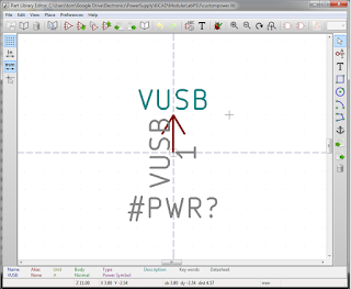
In my design I have an isolated USB interface so I have the USB power and ground which are different from any other power net. I needed to create a VUSB net and USBGND net but how to do it?
Turns out there is a library for power and ground symbols (power). In the library editor you can choose a 'part' from this library and copy/edit it as I described above for the op amps package. I saved this in another library.
When I went back to the schematic sheet I added the library but it didn't appear when I tried to add a power component. It turns out you have to select your custom power components via the parts libraries. Then they work as normal. Confusing? Yes very much so.
During this process I upgraded from 3.X to 4.0RC1 of KiCad and magically my custom power library started turning up when in the power device list.
Another mistake I made is that while I renamed the +5V power device, I didn't rename the pin (the power device is effectively a pin). This meant my VUSB power pin was connected to +5V which (thankfully) got picked up by the DRC. In the image below the blue righting identifies the part name but the grey writing is the pin name. If you right-click and edit the pin you can choose this to be what you want. If you copy another power symbol and don't change this then it will connect everything to the same net!

Footprints
Choosing the footprints all at once is *much* easier than selecting them as you go along. Most of the parts in my project had pretty standard footprints and I could just choose appropriate footprints from the library. I had to be a bit careful with the transistors as depending on the order of their leads there is a different schematic symbol (i.e. for ECB or BCE etc etc). Even the big 63V capacitors were easy as there was a standard footprint that fitted.
Oddly there was no SOT-223 footprint for the surface-mount LM317 I chose. I found a company called Ab2tech that published one on github. I couldn't figure out how to add their library from Git using either the wizard or manually. In the end I just pulled the one footprint I needed, copied this into my project directory and added it.
Many of the footprints I had to create were specified in millimetres. I wasn't sure what to do in regards making them comply with a grid so I decided to just specify their dimensions exactly from the data sheet. Soon find out if this is a problem!
I wasn't sure what size to make holes and pads for through hole parts. I found this guide that said to basically add 0.25mm to the lead diameter for the hole and then add 0.8mm for the pad size. In some cases the pads are carrying high current so I chose to make them a bit bigger again.
Board Layout
Once chose/created all the footprints I exported a net list and imported it into the PcbNew tool. I decided I am probably going to go with Seeedstudio as the board house so I looked up their specs and updated the design rules. The default rules were coarser than Seeed's so I generally left them as is (will change if I need to).
I need to make some of the tracks quite big to handle the current. If you start drawing a trace and then right-click there is a menu for changing the track width but it has no options to select. This is pretty confusing - so how do I change the track width?
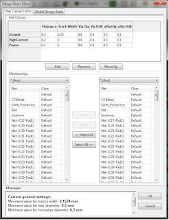
Turns out in the Design Rules dialog KiCAD allows you to define 'classes' of nets and for each class you can define the track width, the via size etc. So I created a high-current, power and regular trace class. I assigned the nets as best I could and began work.
The thing is that not all of a net will have the same amount of current flow. For example the ground connection between the diode bridge and the bulk filter capacitor of a PSU or between the capacitor and the output will definitely need to be thick but the ground going to chip (consuming all of 10uA) will not. This doesn't work very well. Again when I try and change the track width there are no options and I can't.
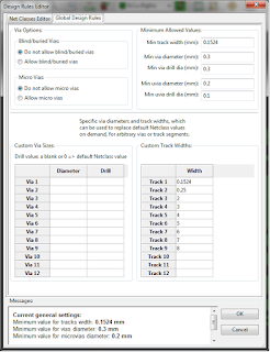
Back to the design rules dialog - on the second tab (Global Design Rules) you can define 'Custom track widths' (you would think there are some standard track widths somewhere but apparently not). If you add some to this list then you can choose them when editing a track!
I need to make some of the tracks quite big to handle the current. If you start drawing a trace and then right-click there is a menu for changing the track width but it has no options to select. This is pretty confusing - so how do I change the track width?
Turns out in the Design Rules dialog KiCAD allows you to define 'classes' of nets and for each class you can define the track width, the via size etc. So I created a high-current, power and regular trace class. I assigned the nets as best I could and began work.

The thing is that not all of a net will have the same amount of current flow. For example the ground connection between the diode bridge and the bulk filter capacitor of a PSU or between the capacitor and the output will definitely need to be thick but the ground going to chip (consuming all of 10uA) will not. This doesn't work very well. Again when I try and change the track width there are no options and I can't.
Back to the design rules dialog - on the second tab (Global Design Rules) you can define 'Custom track widths' (you would think there are some standard track widths somewhere but apparently not). If you add some to this list then you can choose them when editing a track!

The next thing to do is to specify the board outline. Turns out there is a layer called 'Edge.cuts' and if you select this and then select the 'Add graphic line' tool (it's the diagonal dashed line symbol) you can draw the edge of the board.
You then load the netlist generated from the schematic which will dump all the components in a pile somewhere. I moved them off to one side so I could work.
The approach I took was to first place component that had to go in certain places - for example the MOSFETs and regulators that have to go on the heatsink need to be at the back etc. Then I would chose what part of the circuit goes where and slows place components one by one that are related. Basically start with a resistor etc, choose another one that connects to it and place that and so on.
To place a component you hit T and then type in the component designator (C33 for example) and that component appears under your cursor ready to plonk somewhere. Bit annoying if you accidentally pick one up you already placed but hey...
One part of my project is digital so I decided to use a ground plane in that area. There is a tool for this and when you select it and click somewhere it asks what net you want the plane to be and what layer to use. Then you draw the outline of the ground plane and hit end. To begin with nothing happened and after a while I realize it was because there was no ground track on that layer in the region. Just by adding a track into that region it then filled the rest. I make the bottom layer ground plane and the top signals (mostly). Then I added short tracks and via from any components that needed to connect to ground to attach them onto the ground plane. Easy!
No comments:
Post a Comment