I made a couple of small changes and those were :
- I created a circuit to detect CC mode and interfaced this with the micro controller.
- I moved to using a 24V relay as this way I could minimize the heat losses in the regulators feeding the relay circuit.
KiCAD Schematics
First up, here is the the power circuit as drawn in KiCAD

Things to note are the 24V relay I previously mentioned, the 24V regulator that is running off the bias rectifier and the move back to a TO-220 regulator for the 5V line. I worked out that in parallel mode the voltage on the rectified is about 28V which is easily enough room for a 24V regulator. In 40V mode we have even more room. The 24V relay also has a 1.4K coil resistance so this lowers the power loss by even more.
Otherwise the circuit is as before with a transistor switching the relay and another switching the bias regulator between 24V and 40V.
Next is the pre-regulator based on the black-dog design but with the changes to minimize the voltage when the load is low.

Now I have bypassing for the comparator. The circuit that subtracts 3V from the pre-regulator got moved a little as it was easier to draw. Otherwise this is unchanged from the previous design.

The voltage and current regulator design is pretty much as before. I added resistors between the Sense+ and V+ and between Sense- and V- outputs so if the sense lines aren't hooked up the supply will still work.
The other change was the addition of the transistor circuit attached to the output of the voltage controller. The first PNP transistor (Q8) switches off when the output goes within 0.6V of the rail. This occurs when the current limiter has kicked in and the voltage controller is driving the output to the rail to try and get the voltage up to the set point. When the PNP turns off then this turns off Q9 which will send the CCMode line low. Q9 switches the 5V line so the CCMode signal is a 5V logic signal.
Finally the digital control circuit:

As suggested by people on the EEVBlog forum, I used lines to connect signals instead of using labels. I'm not sure this makes it clearer. Otherwise the only change is that I added more bypassing as per the datasheets of the components. This meant a *lot* of additional capacitors as components like the ADUM1201 need two for each side and the micro controller has one for each power pin.
I switched back to using a crystal instead of a ceramic resonator for the ADC as the stability may effect the readings. The MCP2200 USB chip and the ATMEGA328P still use ceramic resonators as they are very convenient.
I added a ferrite to join the digital and analog power nets. This is to stop the digital noise getting back into the current sense circuit (which is also 5V).
PCB
I feel like I have been designing the PCB in my head for weeks. Every time I read a datasheet that has layout guidelines or another paper on bypassing or noise I seem more of the picture.
First I needed to pick a PCB Fab house. PCBShopper helped a lot although in the end I went with SeeedStudio as they seem well supported and popular amongst hobbiest projects. I first made sure that KiCAD was configured with the rules which actually weren't that stringent.
The main things that drive the PCB design are:
- The board needs to be no more than 80 or 90mm wide so I can fit 3 of them on my heatsink side by side.
- The MOSFETs and regulators need to go at the back to go on the heatsink.
- The output needs to go at the front
- The analog and digital sections need to be separate. ADCs and DACs need to be at the edge.
- No ground plane in the analog part - star ground from the current shunt. Ground plane for the digital part.
- No digital lines under analog chips
- Fat traces for current carrying connections.
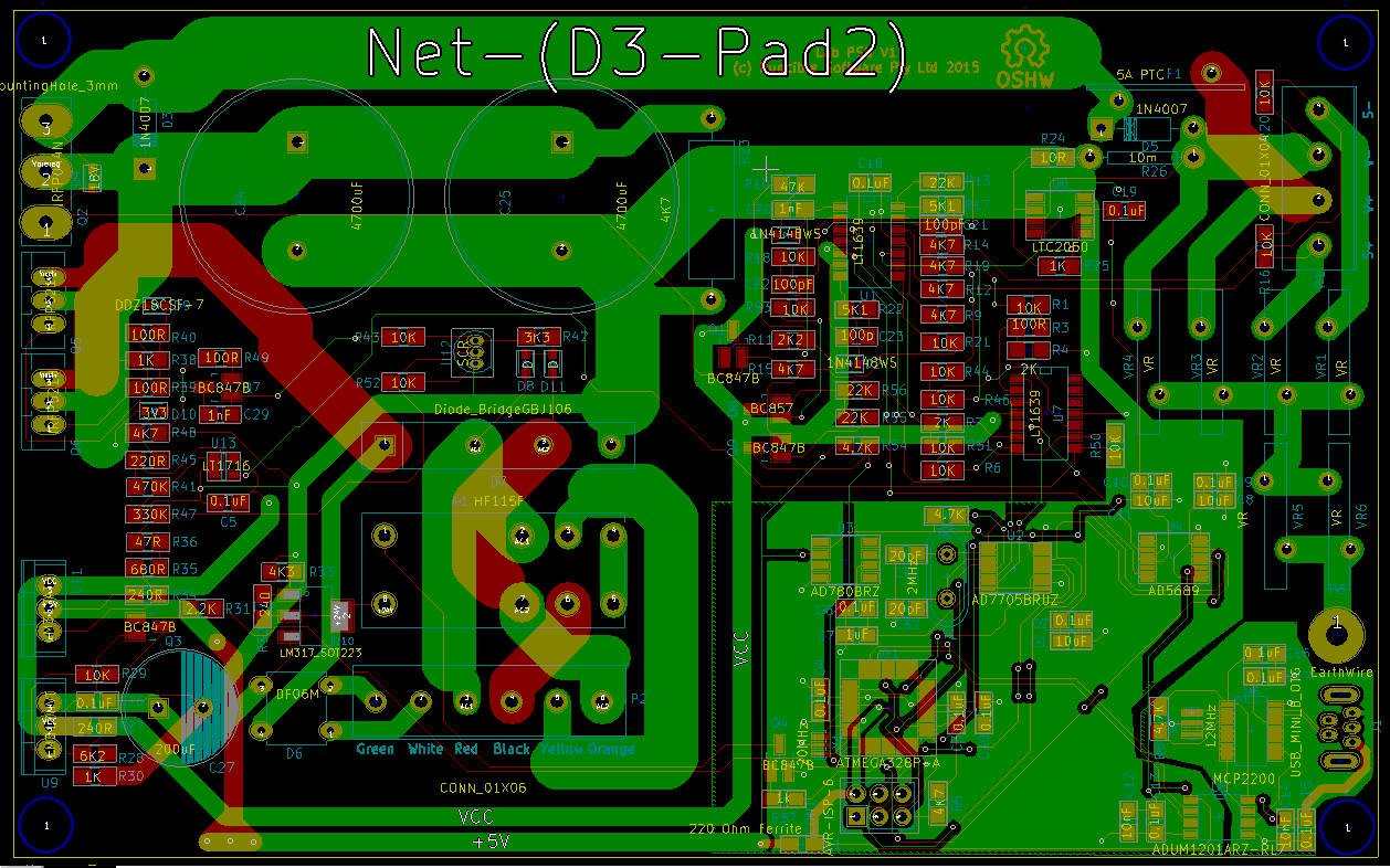
I started by placing the output MOSFET and then the pre-regulator mosfets across the back and then the LM317s. Then I put the capacitors in as they are quite large and need to be close. I figured out the best place for the input connector was in the middle but close to the back and I placed the relay and diode bridge alongside. I put the output connector at the front and all the MOVs along the front edge.
Now I have a small space at the back between the bridge and the MOSFETs for the pre-regulator and power circuits and a larger space at the front for the analog and digital control.
I router the power traces and the pre-regulator. The fat traces proved to be hard. Ideally I would have 10mm traces but 6mm was about the biggest I could really fit.
The pre-regulator was not too hard to place and route. I took the approach of starting with the main component (like a comparator or an op amp) and then starting with one of the resistors/capacitors attached to it. I placed them one at a time and choose the next one connected as I go. I try and line them up in columns (on a 0.5mm grid).
Then I placed the op amps in the analog control circuit and placed/routed the associated components. I left power and ground until last.
I switched to the digital part and after some fiddling decided to place the processor and programming header close together toward the back, then place the USB, USB controller and isolator closer to the front corner. The ADC/DAC go toward the middle (nearer to the analog part).
The digital part was very hack-and-slash compared with the analog routing. I figured out how to make a copper pour and this looked ok. I have a separate copper pour for the isolated USB part also.
The through-hole USB connector was tricky as I needed a *very* fine track to get between the pads. If I don't go between pads then the trace length difference will be too big and it could effect the reliability. This was the one spot where I had to use the minimum track size.
So I stared at it for a few days and tweaked things. In the end I placed an order. Main things I am still not sure about are
- If the bypass capacitors are close enough to the chips. I think this is where using smaller parts would have helped.
- (In hindsight) if I should have put the reference in the analog section away from the digital ground plane.
- I probably should have done a top-side AND a bottom side copper pour in the digital section.
I found this guide useful when exporting the board ready for Seeed. I had no problems getting the fab to accept the board.
Here is the board. Output MOSFET at top left, then pre-regulator MOSFETs below that. The two LM317s for 5V and VCC at bottom and the bulk cap for those nearby. The input connector, relay and diode bridge are in the middle. USB at bottom right, MOVs and ground link above that. Output connector top right. Current shunt and fuse to left of output connector.
So I have ordered the boards and the remaining parts. Now I wait!
No comments:
Post a Comment